High Temperature Cofired Ceramic (HTCC) Hermetic Packages
Multilayer Ceramic Package Capabilities
Electronic Products (EPI) is a powder-to-package, fully integrated HTCC technical ceramics and glass-to-metal package manufacturer. EPI uses a proprietary, advanced ceramics process to create multilayer microelectronic assemblies for harsh environments and conditions.
A multilayer circuit is a type of circuit board that has multiple layers of conductive material, separated by insulating layers. These layers are laminated together to form a single, unified structure. Multilayer circuits are used in a variety of electronic devices, including computers, smartphones, and other types of electronic equipment. They are preferred over single-layer circuits because they can provide more routing channels, reduce the size of the circuit, and improve the overall performance of the device. Multilayer circuits can have anywhere from two to ten or more layers, depending on the complexity of the circuit and the requirements of the device. EPI manufactures custom multilayer ceramic circuits for various applications that require high performance and microelectronic packaging.
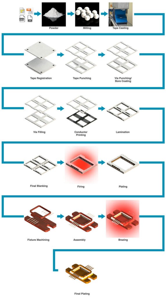
HTCC Ceramic packages follow a multi-stage process to transform a ceramic powder into a tape form. The ceramic tape then follows an extensive process of punching, coating, printing and lamination to prepare it before firing and plating the ceramic package. Each ceramic package is manufactured using it’s own process with our extensive in-house equipment capabilities for maximum efficiency. From prototypes to full production, EPI can support a variety of production volumes.
Ceramic seals and packages give a high level of flexibility to create a microelectronic package in custom footprints while surviving harsh environments. The powder-to-package vertical integration business model allows EPI to control quality, lead-time, and costs to deliver products on time and within budget. Ceramic packages are manufactured in Newburyport, MA under an ISO 9001:2015 quality management system.
We can accept a simple print and most software formats for your prototype design. We are using Solidworks and DraftSight for designing hermetic ceramic packages. Partner with engineers that have mechanical, electrical, and material science expertise to design and manufacture your next requirement for a ceramic seal.
Multilayer Ceramic Package Capabilities
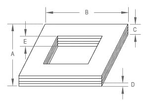
Overall Dimensions – inches [mm]
| Standard | Custom | |
|---|---|---|
| Maximum Size (A x B) | 2 x 2 [50.8 x 50.8] | 3 x 3 [76.2 x 76.2] |
|
Tolerance (As fired)
|
±1%, NLT ±.005 [0.127] |
±0.5%, NLT ±.003 [0.076] |
|
Number of Layers (C)
|
2 |
10 |
| Cavity Depth | 0.040 [1.00] typ. | Up to 0.120 [3.00] |
NLT -Not Less Than
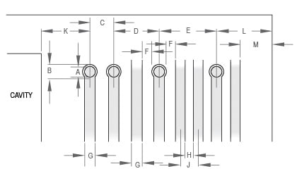
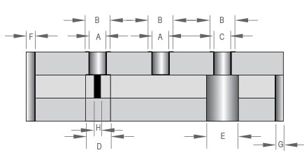
Via & Conductor Dimensions (Tape Layers)
| Standard ° | Custom | |
|---|---|---|
| A. Via Hole Diameter | 0.010 [0.254] | 0.006 [0.152] |
| B. Via Cover Dot Diameter | 0.020 [0.508] | 0.012 [0.305] |
| C. Via Center Spacing | 3 x Θ | 3 x Θ |
| D. Via Center Spacing | 3 x Θ + G | 3 x Θ + G |
| E. Via Center Spacing | 3 x Θ + 2G + H | 3 x Θ + 2G + H |
| F. Via Cover Dot to Line Clearance | 0.012 [0.305] | 0.008 [0.203] |
| G. Line Width | 0.010 [0.254] min. | 0.005 [0.127] min. |
| H. Line to Line Clearance | 0.010 [0.254] min. | 0.006 [0.152] min. |
| J. Line Center Spacing | 0.020 [0.508] min. | 0.011 [0.279] min. |
| K. Cavity to Via Center | 3 x Θ | 2.5 x Θ |
| L. Outside Edge to Via Center | 4 x Θ | 3 x Θ |
| M. Line to Outside Edge | 0.020 [0.508] | 0.015 [0.381] |
° = Greater Dimension Available
Coated Via Hole Dimensions (Tape Layer)
| Standard ° | Custom | |
|---|---|---|
| A. Closed Hole Diameter | 0.020 [0.508] min. | 0.015 [0.381] min. |
| B. Via Cover Dot Diameter | 0.020 [0.508] | 0.014 [0.356] |
| C. Open Hole Diameter | 0.020 [0.508] min. | 0.015 [0.381] min. |
| D. Via Cover Dot Diameter | 0.020 [0.508] (Same as B.) | 0.014 [0.356] (Same as B.) |
| E. Opening Diameter | 0.020 [0.508] min. | 0.015 [0.381] min. |
| F. Castellation (Chip Carrier) | Θ0.020 [0.254] radius | Θ0.015 [0.381] radius |
| G. Castellation (Chip Carrier) | Θ0.020 [0.254] radius | Θ0.015 [0.381] radius |
| H. Solid Via Diameter | Θ0.006 – 0.15 [0.152 – 0.381] typ. |
° = Greater Dimension Available
Material Properties and Plated Metallizations
Alumina and Aluminum Nitride Properties
| 92% Alumina (Al2O3) | 94% Alumina (Al2O3) | 99.8% Alumina (Al2O3) | Zirconia Toughened Alumina (ZTA) | Aluminum Nitride (AlN) | |
|---|---|---|---|---|---|
| Color | Black | White | White | White | Gray |
| Crystal Size (µm) | 8 | 8 | 8 | 6 | 5 |
| Water Absorption (%) | 0 | 0 | 0 | 0 | 0 |
| Density (g/cc) | 3.67 | 3.67 | 3.91 | 4.3 | 3.3 |
| Hardness (V) | 12 | 13 | 15 | 14.5 | 11.5 |
| Fracture Toughness (MPam^0.5) | 3~4 | 4~5 | 3~4 | 6 | 3 |
| Flexural Strength (MPa) | 630 | 430 | 450 | 640 | 290 |
| Modulus (GPa) | 320 | 320 | 380 | 338 | 330 |
| Compressive Strength (MPa) | 1800 | 2200 | 2300 | 2800 | 2100 |
| CTE (x10-6/°C) | 7 | 7 | 6.5 | 6 | 4.5 |
| Thermal Conductivity @25°C (W/mK) | 20 | 25 | 30 | 25 | 180 |
| Specific Heat (J/gK) | 0.79 | 0.78 | 0.79 | – | 0.72 |
| Dielectric Strength (KV/mm) | 12 | 16 | 16 | 14 | 16 |
| Dielectric Constant (@ 1MHz) | 10 | 9.5 | 10 | 12.4 | 8.5 |
| Dielectric Constant (@ 1GHz) | 10 | 9.5 | 9.6 | 9.5 | 8.4 |
| Dielectric Loss (@ 1MHz) | 0.0013 | 0.003 | 0.001 | 0.005 | 0.005 |
| Volume Resistivity | >1014 | 1014 | 1014 | 1014 | 1014 |
Tungsten Properties
| Tungsten | |||||
|---|---|---|---|---|---|
| Bulk Modulus (GPa) | 310 | ||||
| Shear Modulus (GPa) | 161 | ||||
| Melting Point | 3410°C ±30ºC | ||||
| Boiling Point | 5500ºC | ||||
| CTE (x10-6/°C) | 4.5 | ||||
| Adhesion | 4.3K g/mm2 (6,000 psi) | ||||
| Solder Leach | 10 Cycles – No Degradation of Nickel Over Tungsten (30 Seconds Dipping Per Cycle in 60/40 @ 230°C) | ||||
| Thermal Conductivity @25°C (W/mK) | 150-160 | ||||
| Electrical Resistivity | 5.5 x 10⁻⁸OΩ per cm | ||||
| External Sheet Resistivity (plated) | 5mΩ/square | ||||
| Internal Sheet Resistivity | 10mΩ-12mΩ/square | ||||