TO Packages: Headers, Caps, Lids, and More
From legacy transistor outline packages to new, custom hermetic packages


Transistor outline (TO) packages have created an industry standard footprint to design and manufacture instrumentation, sensors, and devices. Electronic Products (EPI) is an expert designer and manufacturer of both legacy and custom engineered, JEDEC-compliant TO packages and headers. With over 60 years-worth of custom and standard TO packaging experience, we’re ready to handle every challenge from matching legacy transistor packages to designing a state-of-the-art optical sensor package.
EPI is a high-quality alternative to other manufacturers and suppliers who are not specialists in TO styles, offering quick delivery of both matched seal and compression seal TO packages and headers from our U.S. facility and headquarters in Newburyport, Massachusetts. Our TO designs are trusted to be 100% hermetic packages that perform reliably under the harshest conditions.


Matched seals typically use CTE-matched ASTM-F15 Alloy (Kovar) and CTE-matched glass compositions to create a seal. Compression seals rely on metals like plain carbon steel 1010 and ASTM-F30 (Alloy 52), which have higher CTE, to compress the glass during the cooling phase of the fusing process. In addition to our glass-to-metal seal technologies, we offer ceramic-based designs for more complex optoelectronic packages.
EPI provides TO packages and headers with a plating finish exact to customer specifications. These finishes include: nickel (Ni), copper (Cu), silver (Ag), and gold (Au), and combinations. For our optical customers we can also provide clear flat or convex lenses.
BENEFITS
- In-house design expertise in hermetic packages, material science, and industry applications
- Standard, JEDEC-compliant outlines available for drop-replacement or new designs
- Variety of plating materials with ability to combine for optimal performance
- Optional compression or matched seal construction based on application
- ISO 9001:2015 US manufacturer
- RoHS / REACH-Compliant packages
PLATING MATERIALS
- Nickel (Ni)
- Copper (Cu)
- Silver (Ag)
- Gold (Au)
- Combination of above plating materials
Image Library
TO-66 9-pin hermetic seal no background
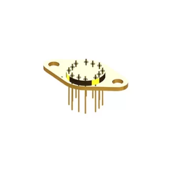
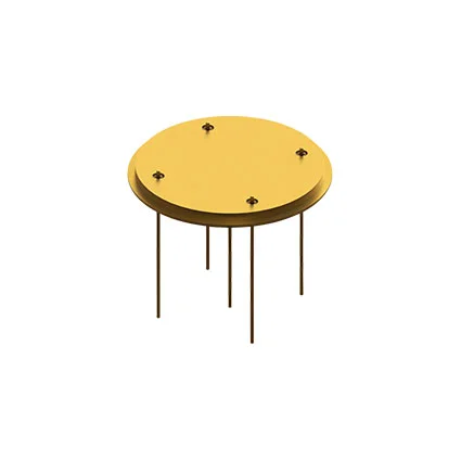
TO-66 12-pin hermetic seal
TO-46 ceramic detector package
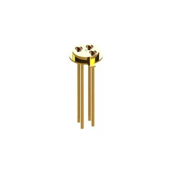
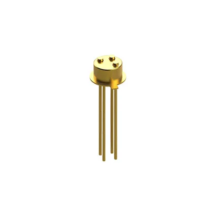
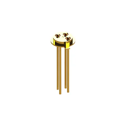
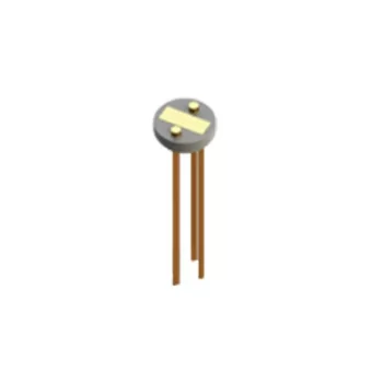
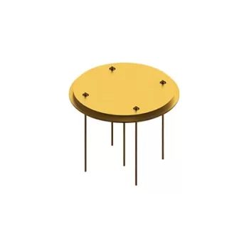
TO-46 hermetic header with 3+1 configuration
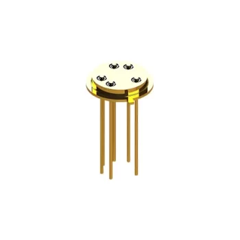
TO-39 hermetic header with 5+1 configuration
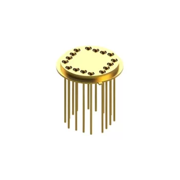
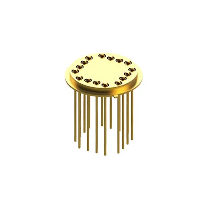
TO-8 16-pin hermetic seal
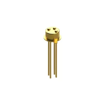
TO-18 hermetic header with 3+1 configuration
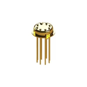
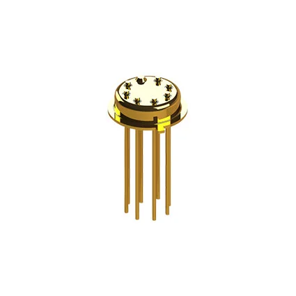
TO-5 hermetic seal with 7+1 configuration
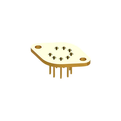
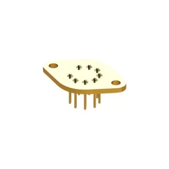
TO-8 header jumbo package
FAQ
WHAT IS A TRANSISTOR OUTLINE?
The Transistor Outline or “TO” package was developed by the semiconductor and microelectronics industry in the 1950s. In addition to addressing requirements for very low thermal resistance, the goal was to create highly reliable (often hermetic) packages in common outlines to keep costs down while standardizing a suite of solutions in accordance with JEDEC . (While there are plastic versions of TO packages, this article pertains to metal TO packages.) The basic TO or “metal can” package consists of a metal base with leads exiting through a glass seal. This glass seal can be a compression seal or a matched seal. After device assembly in the package, a metal lid is resistance welded to the metal base forming the hermetic seal. These packages usually contain less than 24 leads.
WHAT ARE SOME POPULAR TO PACKAGES?
One of the most popular TO packages, the TO-3, was originally designed by Motorola c. 1955. It features lead spacing that was designed to allow plugging the device into a common socket used by Motorola at that time. But it largely remains the same today. It provides low thermal resistance for hermetically packaged voltage regulators, power transistors, rectifiers, and other integrated circuits. Another popular package is the TO-8. This style is popular in the RF/microwave industry for housing oscillators, and in the optical industry for housing sensors. TO-39, TO-5, TO-18, and TO-46 are some of the most commonly configured TO headers at EPI.
WHAT ARE THE TYPES OF TO HEADER APPLICATIONS?
TO packages and headers are in use today in all facets of microelectronic applications on both the transmit and receive side of a transceiver system. They’re also proven in high-speed data transfer, infrared, and other opto-electronic applications. Micro-Electro-Mechanical Systems (MEMS) packaging represent a new area of microelectronic packaging applications for the TO package. MEMs systems enable optical signals to be switched using a range of small, mobile mirrors and are becoming increasingly accepted in high volume applications such as LCD projectors. Various sensor types to measure pressure, temperature, humidity, and vibration also utilize TO headers to isolate the sensing element, protect electronics, and transmit signal.
WHAT ARE EXAMPLES OF A CUSTOM TO HEADERS?
EPI manufactures a customized TO header with up to 14 holes; typically a TO-5 has 1 to 8 positions. This creates a high density hermetic feedthrough package in a compact design. TO-8 headers are available with up to 16 pins.
In various configurations, EPI can machine in a weld projection to simplify the mechanical connection to the TO header.