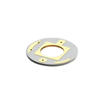
Optical / Optoelectronic Packages
Hermetic optical packages designed in small footprints with complex circuit capabilities
Product Categories
-
RF & Microwave Packages
-
Optical / Optoelectronic Packages
-
Power Discrete Packages
-
TO Packages: Headers, Caps, Lids, and More
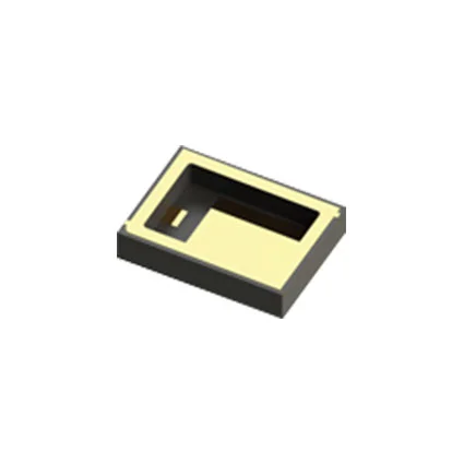
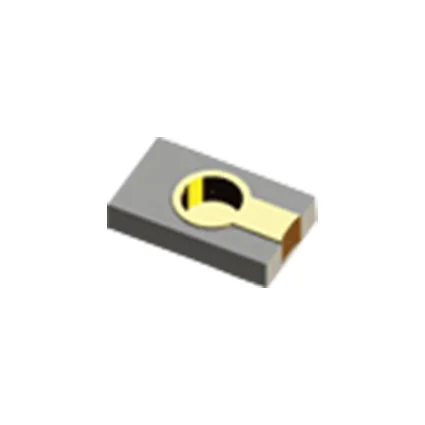
Electronic Products (EPI) is your resource for a variety of optical and optical electronics packages. Our in-house glass-to-metal and ceramic capabilities as well as design expertise allow you the freedom to choose from any one of several standard optical package designs or choose to have us design a unique package for your custom optical device application. EPI manufactures some of the smallest footprint, hermetic, ceramic-based Pill packages for VCSEL, LEDs, and a variety of sensing elements.
Our designs enable compact optoelectronic packages to meet fit, form, and function in new sensing applications in harsh environments. EPI also designs and manufactures large, multilayer, high I/O, aluminum nitride (AlN) based substrates for the most demanding focal plane arrays used in applications such as image sensing and LiDAR. We specialize in providing robust solutions for military, aerospace, and commercial sensing applications.
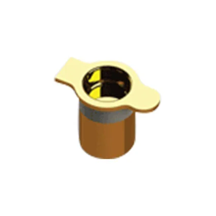
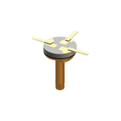
EPI offers both traditional TO header glass-to-metal seals as well as ceramic-based optical TO-header packages to enable more complex circuit patterns in optoelectronic devices. Our optoelectronic packages are designed for a variety of industries and production volumes. With a vertically-integrated powder-to-package process, our optical packages maintain high quality and competitive lead times.
CUSTOMIZATION CAPABILITIES
- Multi-layer circuits
- Increased power capacity
- Expanded temperature range
- “Pill” package footprints
KEY BENEFITS
- Small footprints
- Ability to manufacture custom, multilayer assemblies
- Designed and manufactured in Newburyport, MA
- ISO 9001:2015
- Glass-to-metal and ceramic seal technologies to find most suitable for application
TYPES OF OPTICAL PACKAGES
- TO Headers
- Components
- VCSEL
- LED
- Sensors
- Substrates
- Windows
- Lenses
Image Library
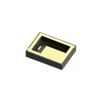
AIN SMD.22 hermetic power package U4 layout
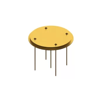
TO-8 header jumbo package

Ceramic pill pack header package
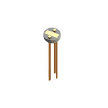
TO-46 ceramic detector package
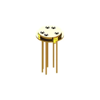
TO-39 hermetic header with 5+1 configuration
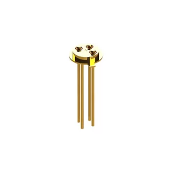
TO-46 hermetic header with 3+1 configuration
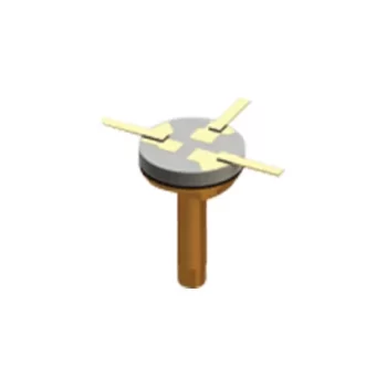
Custom TR switch hermetic package
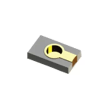
Hermetic seal for surface mount emitter detector
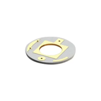
Ceramic TO header hermetic substrate
FAQ
WHAT ARE OPTOELECTRONIC PACKAGES?
Optoelectronic packages are specialized components that are used to protect and preserve the integrity of optoelectronic devices and systems. Optoelectronic devices are devices that use light or other electromagnetic radiation to transmit or detect information, and are used in a variety of applications, including communication, sensing, and imaging.
Optoelectronic packages are designed to provide a protective enclosure around the optoelectronic device or system, and are typically made from materials that are transparent or semi-transparent to the electromagnetic radiation being used by the device. They are often made from materials such as glass, quartz, or plastic, and may also include additional components such as lenses, filters, and reflectors to control the transmission and detection of the electromagnetic radiation.
WHAT ARE COMMON OPTOELECTRONIC APPLICATIONS?
Optoelectronic packages are commonly used in a variety of applications, including communication systems, sensors, and imaging systems. They are an essential component of many optoelectronic devices and systems, and play a critical role in protecting and preserving the integrity of these systems.
WHAT IS A VCSEL?
A Vertical-Cavity Surface-Emitting Laser (VCSEL) is a type of semiconductor laser that is used in a variety of applications, including communication, sensing, and imaging. VCSELs are characterized by their ability to emit light vertically from the surface of the device, rather than from the edge of the device as is the case with traditional lasers. VCSELs are made using a variety of semiconductor materials, including gallium arsenide and indium phosphide, and are typically fabricated using microelectronic fabrication techniques. They are highly efficient and reliable, and are able to operate at high speeds and over a wide range of temperatures. VCSELs are commonly used in a variety of applications, including fiber optic communication systems, data storage systems, and medical diagnostic systems. They are also used in a variety of sensing and imaging applications, including industrial inspection, security systems, and environmental monitoring.
WHAT IS A MULTILAYER CIRCUIT?
A multilayer circuit is a type of circuit board that has multiple layers of conductive material, separated by insulating layers. These layers are laminated together to form a single, unified structure. Multilayer circuits are used in a variety of electronic devices, including computers, smartphones, and other types of electronic equipment. They are preferred over single-layer circuits because they can provide more routing channels, reduce the size of the circuit, and improve the overall performance of the device. Multilayer circuits can have anywhere from two to ten or more layers, depending on the complexity of the circuit and the requirements of the device. EPI manufactures customized multilayer circuits using advanced ceramic processing to enable high-density microelectronic designs.
WHAT IS ALUMINUM NITRIDE (AIN)?
Aluminum nitride (AlN) is an inorganic compound that is composed of aluminum and nitrogen. It is a white, high-strength, and high-thermal-conductivity material that is widely used in the electronics industry as a substrate for microelectronic devices such as integrated circuits (ICs) and high-brightness light-emitting diodes (HB-LEDs). AlN has a number of attractive properties for these applications, including a high melting point, good electrical insulation, and a low coefficient of thermal expansion. It is also resistant to corrosion and can be easily machined into complex shapes.

